Services
The Keck Lab offers a variety of services.
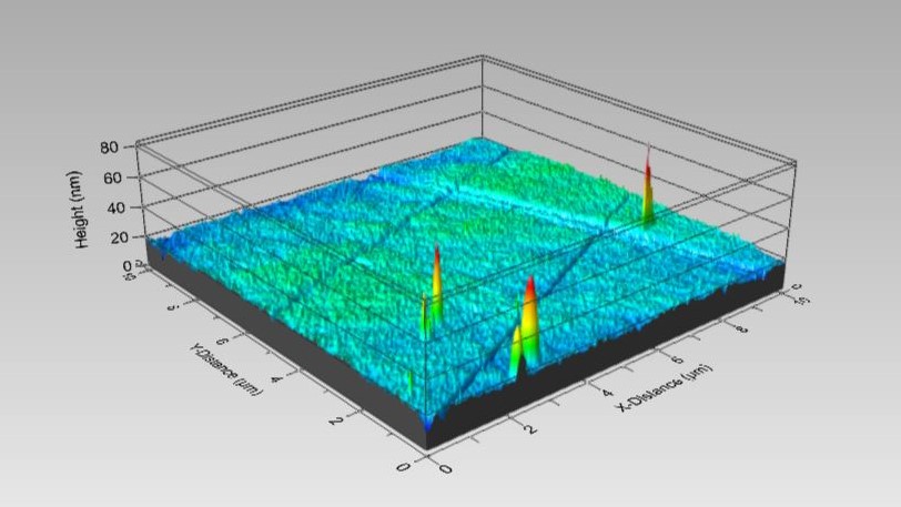
Surface Metrology Characterization
Characteristics such as surface roughness, step heights, and feature dimensions can be determined. Sample images can also be taken using the SEM or optical microscopes.
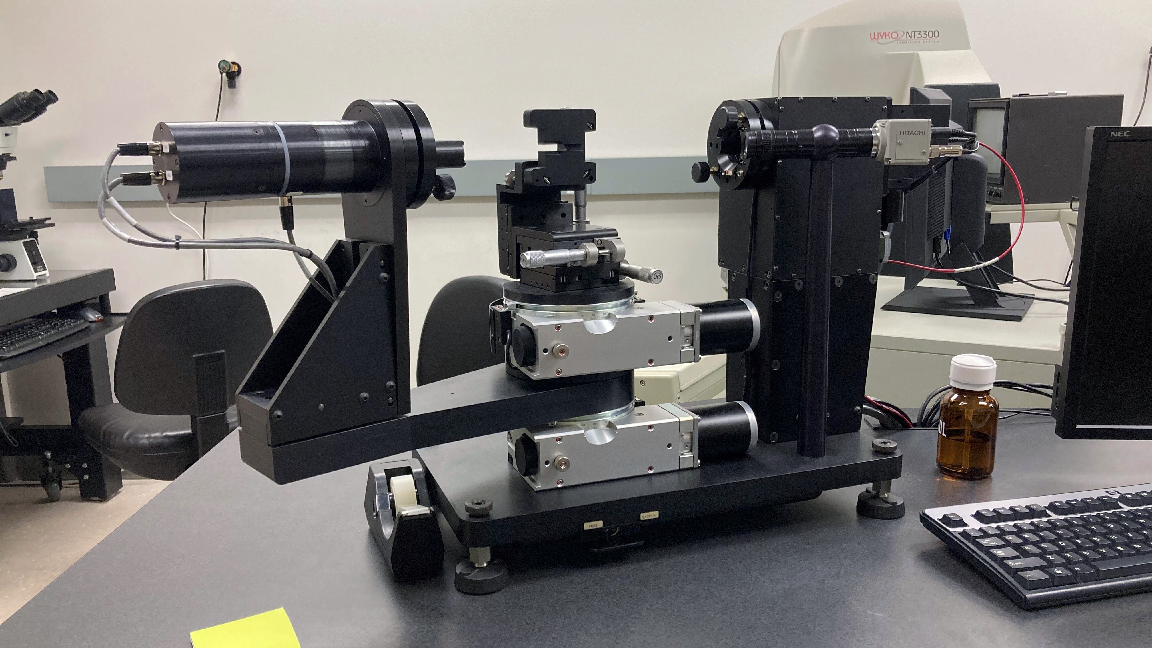
Optical Properties Characterization
Characteristics such as transmissivity, reflectivity, optical constants, emission spectrum, and optical layer thickness can be measured across a wide range of incidence angles and wavelengths.
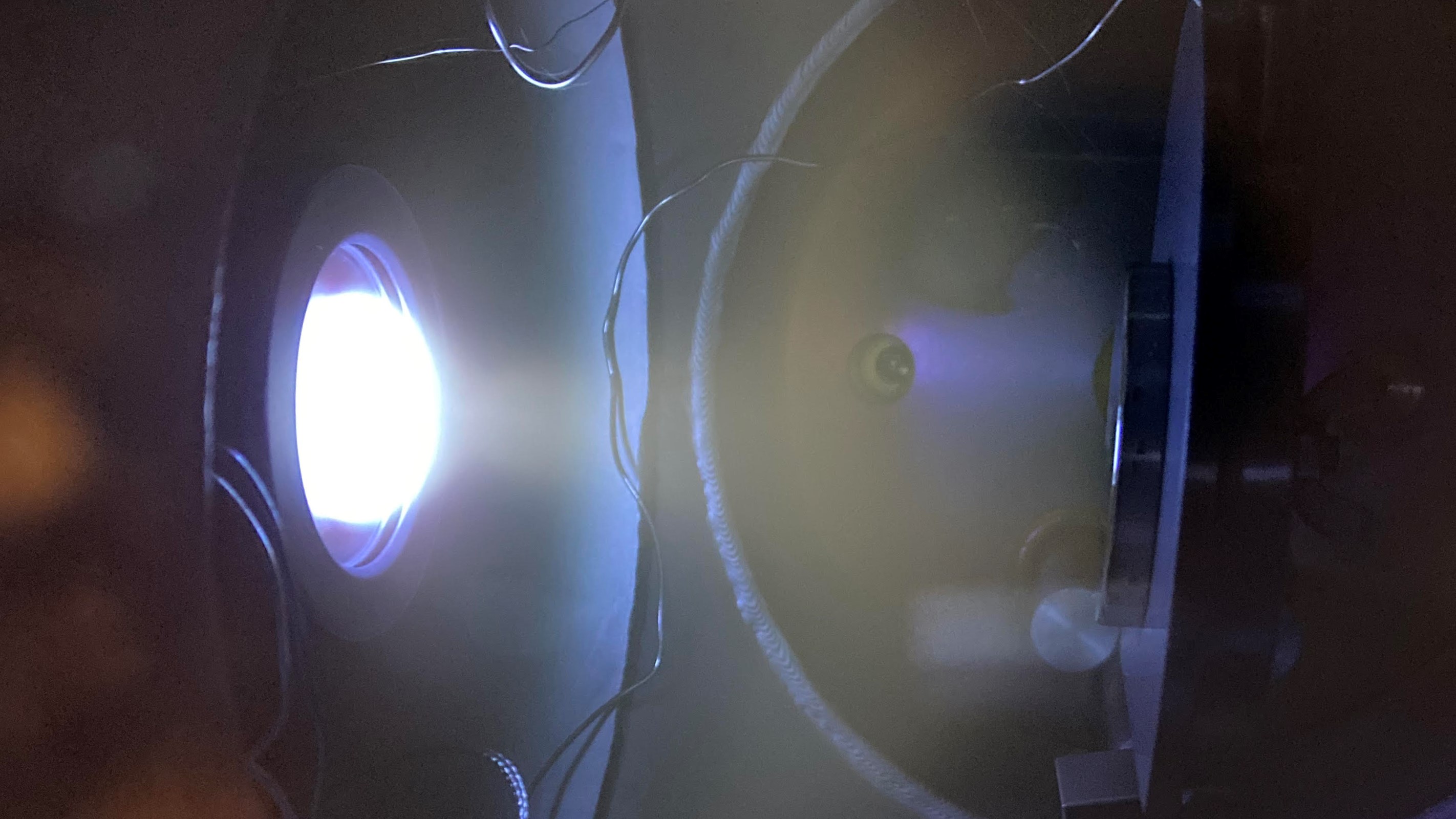
Metal/Dielectric Coatings
Samples can be coated in a wide variety of dielectric and metal materials using sputtering or thermal/e-beam evaporation.
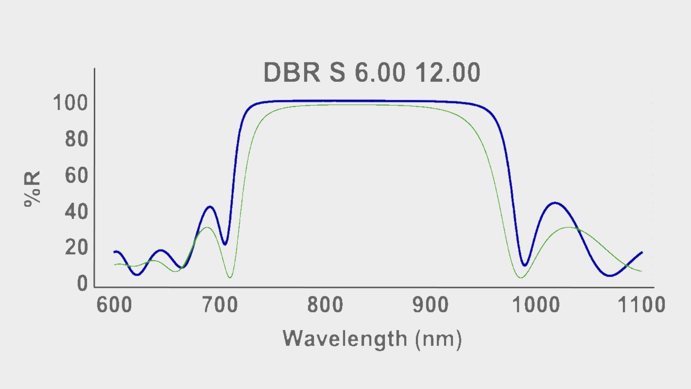
Optical Coating Design and Fabrication
Certain optical coatings can be designed and fabricated for specific use cases by depositing films onto a substrate. Examples include mirrors, DBRs, and bandpass filters.
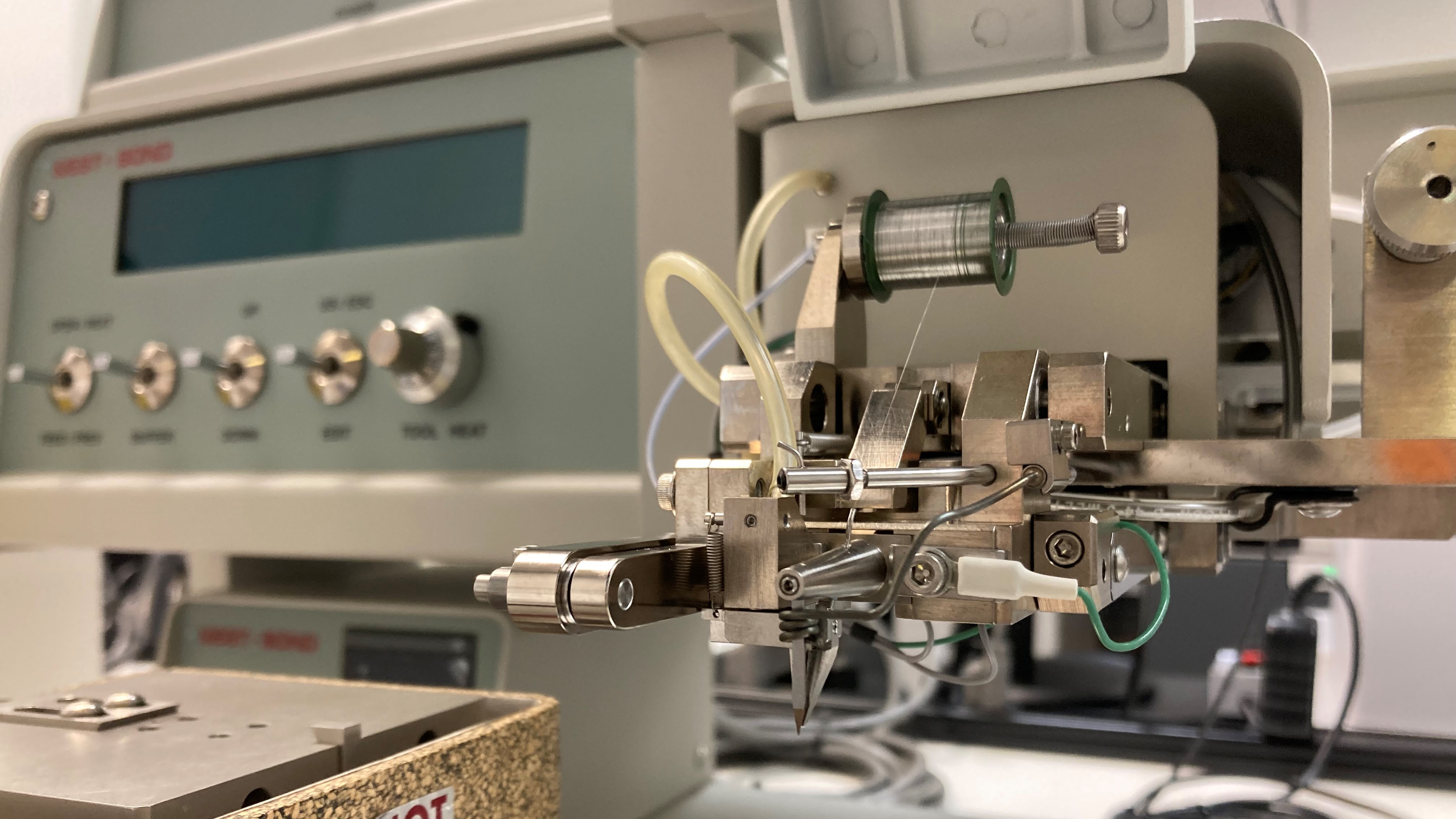
Microfabrication Services
Certain photolithography and wire bonding capabilities are available. Wafer size is limited to a maximum of 3".
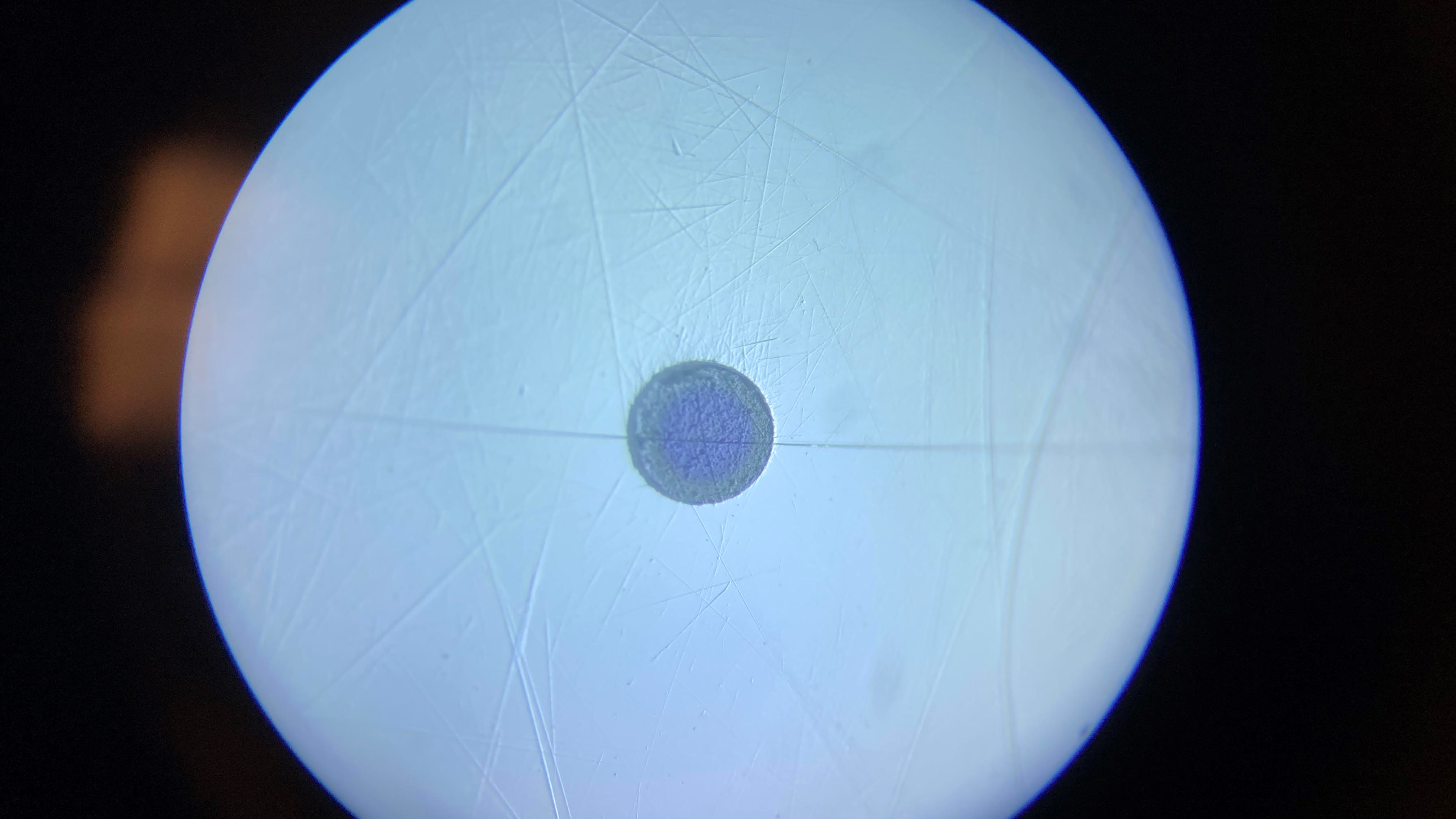
Fiber Optic Services
Fiber optic services include connector replacement, fiber polishing, and fiber splicing.
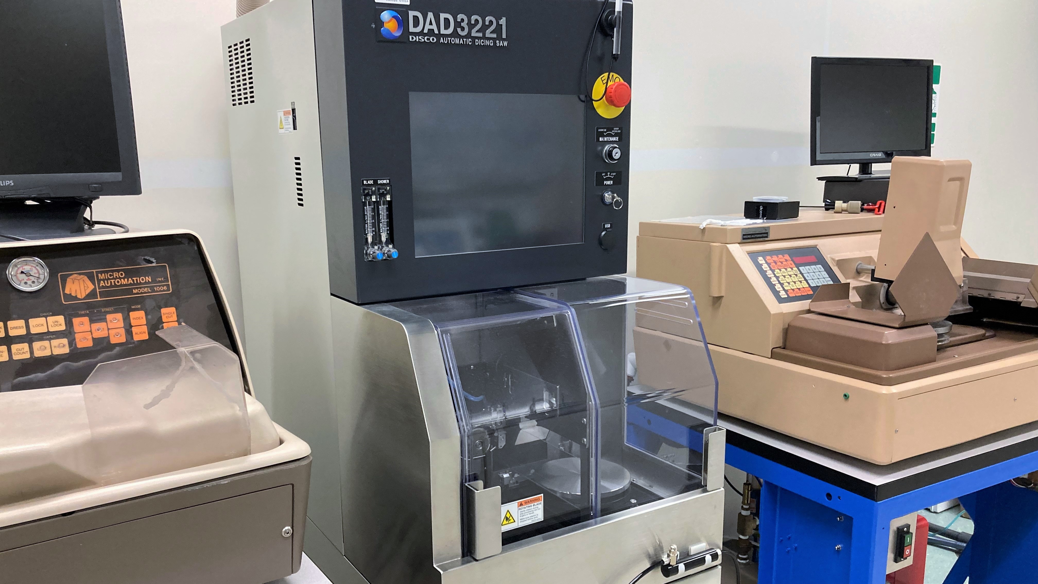
Dicing
Dicing is available for a variety of substrates. Workpiece size is limited to a maximum diameter of 4".
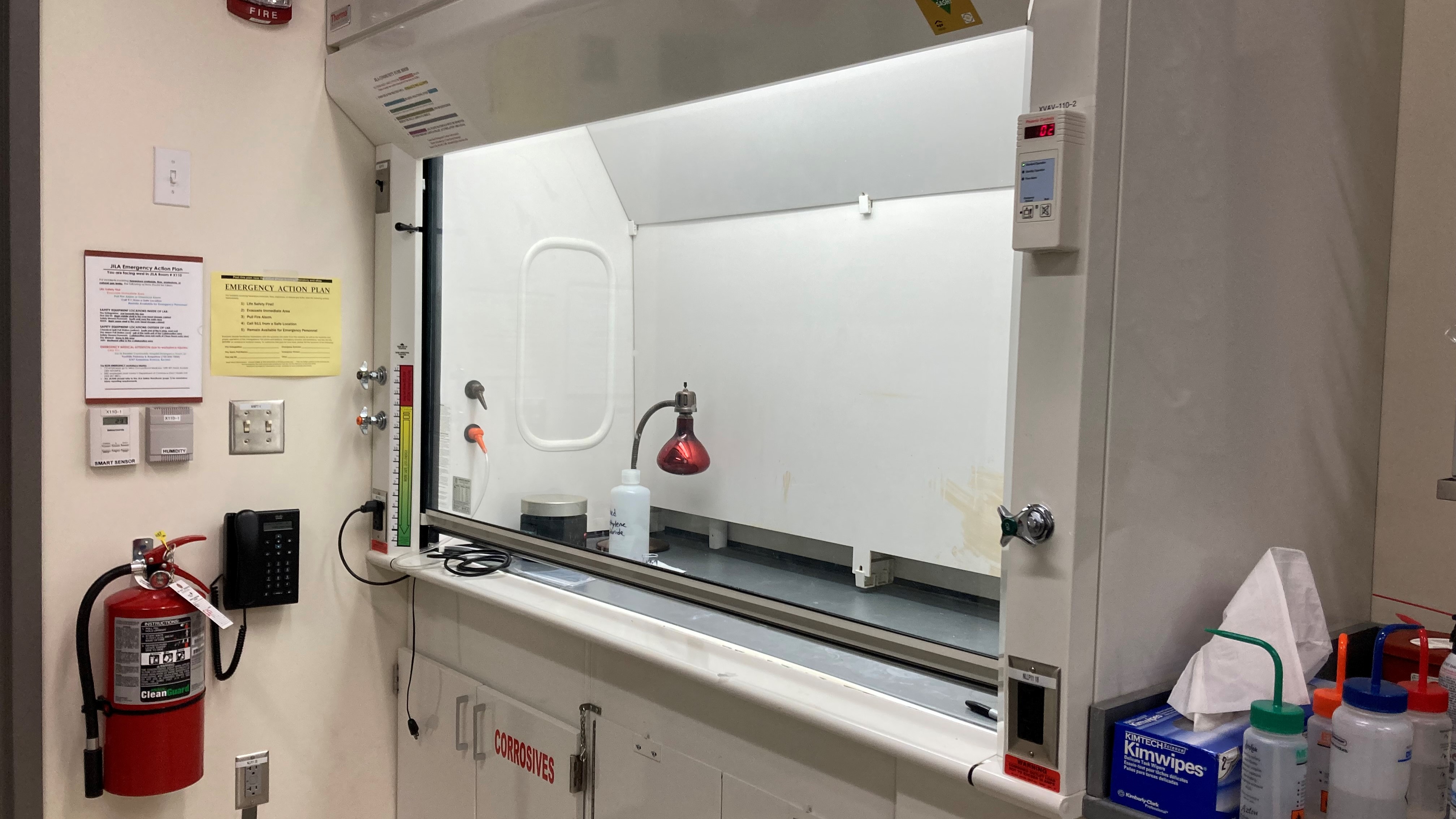
Chemistry
Assistance can be provided for certain chemistry processes. The Keck Lab reserves the right to refuse specific chemicals on lab premises.
Request a Service
If you have a potential job, please contact us to discuss further details. This includes scope, specifications, custom accomodations, labor time estimates, and timeline.
Tutorials
The Keck Lab requires instruction in the operation of all instruments, tools and software in the lab. The tutorials are given on an as-needed basis.
